-
Notifications
You must be signed in to change notification settings - Fork 8
Home
4 channel GS/s DDS EEM
Design files (schematics, PCB layouts, BOMs) can be found at Urukul/Releases. A self-contained datashet is available from M-Labs
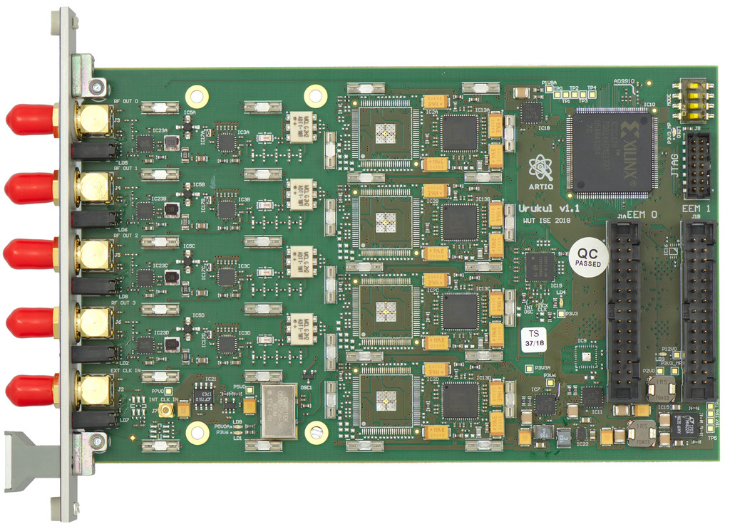
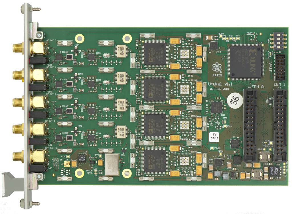
Urukul is a 4 channel DDS-based frequency synthesizer for the EEM form factor. It provides sub-Hz frequency resolution, controlled phase steps, and accurate output amplitude control.
- Two variants of Urukul are available with different DDS chips: AD9912 and AD9910
- Output frequency (-3 dB): <1 to >400 MHz
- Frequency resolution:
- Frequency update rate using the single-width SPI bus: > 500 kHz burst aggregate, TBC
- Phase offset resolution: 14 bit (AD9912), 16 bit (AD9910)
- Digital amplitude (ASF) resolution: 14 bit (AD9910 only)
- DAC full scale current resolution: 10 bit (AD9912), 8 bit (AD9910)
- DAC full scale current slew rate: ~6 mA/20 µs, 100 ns/LSB (AD9912) #205
- Temporal resolution, FTW/POW/ASF updates: 4 ns (IO_UPDATE on a SERDES TTLOut) (TBC)
- OSK: not supported
- DRG control pins: not supported
- Profile (using the AD9910 PROFILE pins): ganged and exposed in the shift register
- Anti-Aliasing: The lowpass can be replaced by a custom discrete filter. This allows usage of the second or third Nyquist zones.
- Digital step attenuator resolution: 0.5 dB
- Digital step attenuator range: 0 to -31.5 dB
- Digital step attenuator glitch duration: 100 ns
- Nominal max output power (1dB compression from expected attenuator/ASF/FSC setting due to pre-amplifier): 10 dBm
- Temporal resolution RF switch: 1 ns (limited by FPGA OSERDES/ARTIQ TTLOut resolution)
- RF switch speed: 100 ns rise to 90 %
- RF switch isolation: 70 dB
- Jitter RF switch: < 1 ns, TBC
- RF switches controlled by dedicated LVDS lines on EEM1 and by shift register (logical OR)
- Crosstalk: -84 dB with victim RF switch open, -110 dB with victim switch closed
- Cross-channel-intermodulation: -90 dB
- Harmonics: at 6 dBm: -40 dB, -54 dB; at 10.5 dBm: -34 dB, -28 dB
- Phase noise/stability (100 MHz ref in, 1 GHz DDS PLL, 81 MHz output):
- 0.1 Hz: -85 dBc/Hz
- 1 Hz: -95 dBc/Hz
- 10 Hz: -107 dBc/Hz
- 100 Hz: -116 dBc/Hz
- 1 kHz: -126 dBc/Hz
- 10 kHz: -133 dBc/Hz
- 100 kHz: -135 dBc/Hz
- 1 MHz: -128 dBc/Hz
- 10 MHz: -149 dBc/Hz
- AM-to-PM coefficient: < 5 deg/dB (TBC)
- Amplitude temperature coefficient: < 0.01 dB/K TBC
- Amplitude noise/stability: TBD
- RF switch turn-on chirp: <0.1 deg/s (excluding the first ~µs)
- Input frequency: 10 MHz to 1 GHz (TBC, depending on PLL/clocking configuration)
- Input power: 10 dBm nominal (TBD to TBD dBm)
- Source: External SMA, internal MMCX (from Kasli or Clocker), or on-board XO
- Selection between MMCX and XO: on board jumpers
- Selection between MMCX/XO and SMA: software
- Default design is 1 GHz DDS clock from 125 MHz or 100 MHz reference frequency input using the DDS PLLs
- On-board divider divides the input clock by 1, 2 or 4 (programmed by the CPLD). Default is 1 for the AD9912, 4 for the AD9910.
- AD9912 PLL 11 - 200 MHz (2.75 - 800 with 1/4 divider), 4x - 66x ratio even
- AD9910 PLL accepts clocks between 3.2MHz and 60MHz (12.8 and 240 with divider), PLL multiplication factors between 12 and 127 (48 and 508 with divider)
- Air flow: > 50cm/s (from thermal simulation, #321), TBD
- Power consumption: 7 W (AD9910)/6.5 W (AD9912) with 1 GHz PLL, 4x400 MHz, 10.5 dBm, 52 C DDS temperature sitting on bench
- Each channel:
- SMA RF output
- Green LED indicating RF output enabled
- Red LED indicating DDS sychronization/PLL error or software-controlled function
- One SMA for the reference frequency input, up to 1 GHz
- Red LED: over temperature
- Green LED: power good
v1.4+ boards from Creotech are thoroughly tested using their test bench. Here is an example v1.4 report.
Urukul has deterministic phase control in the sense that phase jumps are well defined and deterministic in their jump size.
Phase control beyond that level requires aligning the synchronization clock phase to the other DDSs on a card and more importantly to the RTIO timebase. The different approaches are detailed below. Only the AD9910 active SYNC approach has been implemented.
DDS_RESET provides a way to deterministically reset all AD9912 DDS SYNC_CLK dividers (see a corresponding ADI discussion). It remains to be seen whether this also works when using the PLL. If it does not, the AD9912 variant can only made absolutely synchronous when not using the PLL.
DDS_RESET needs to be well timed w.r.t. DDS SYSCLK (meet S/H). That requires determination of the timing t_RESET of DDS_RESET w.r.t. DDS REFCLK/SYSCLK. This which will need to be measured manually, computed using cable lengths and empirical offsets, or always found empirically using a measurement of phase update determinism when scanning a delay. From the timing t_RESET the proper timing t_UPDATE or IO_UPDATE w.r.t. SYNCCLK can be inferred. The latter should only be required once for a given hardware design.
Using the AD9910 SYNC circuitry, a marker signal (SYNC) is distributed to all DDS that resets their SYNCCLK dividers. If SYNC originates from the FPGA (Kasli/Sayma/Metlino), then the delay of SYNC_OUT w.r.t. REFCLK/SYSCLK needs to be reproducibly adjusted. This is done using the DDS-internal delays seeded with a persistently stored initial value (start with last value, optimize it, and store it for next optimization after reboot).
Given this synchronization the proper timing t_UPDATE or IO_UPDATE w.r.t. SYNCCLK can be inferred. The latter should only be required once for a given hardware design.
In this mode SYNC would be driven by the first DDS and emitted from Urukul to the FPGA. On the FPGA it would be used to re-time IO_UPDATE (or PROFILE) with respect to SYNC CLK and thus SYSCLK. The requirement on reproducibly adjusting the latency (from RTIO clock to DDS/SYNC domain) are similar to AD9910 active SYNC with the exception that the FPGA needs to perform delay adjustment as well now.
This mode does not place the IO_UPDATE timing reproducibly w.r.t. RTIO clock. It only ensures that IO_UPDATE/PROFILE always meets S/H w.r.t. DDS SYNCCLK.
The IO and logic router on the Urukul CPLD controls the SPI buses, multiplexes the different chips, and implements the shift register for control of miscellaneous functionality.
Its implementation and functionality are documented in the CPLD source code.
For an Urukul board that is not delivered as part of a prebuilt system, the CPLD may need to be configured before use. See the Firmware page for more information.
Urukul operates from one or two EEM connectors. In standard SPI mode, the complete Urukul functionality can be accessed using only that interface. Standard SPI mode only needs the second EEM connector to interface with high resolution RF switching and synchronization signals. SU-Servo mode always requires two EEM connectors. Details are documented in the CPLD source code.
Urukul can be integrated with Sampler to form a multi-channel, multi-profile digital servo controller. Support for this is built into Artiq. The legacy development repository can be found here.
Scientific papers where Urukul was used:
Dynamical low-noise microwave source for cold atom experiments, B. Meyer et al.
Urukul v1.2 and v1.3 have design flaws; see this Issue. Many labs successfully use unmodified v1.2 and v1.3 boards in ongoing research. Several patches patch2019 are recommended to increase the stability of RF output and decrease the likelihood of component failure, though they do not extend the functionality of the hardware.
Urukul v1.4 was released to production 9/27/2019.
- The change log is here.
- Urukul 1.4 moved to a larger CPLD vs previous versions. This is among the reasons that the CPLD gateware for hardware v1.4 is not compatible with hardware versions v1.1, v1.2, v1.3.
Urukul v1.5 was released to production 2/19/2020.
- The change log is here.

