-
Notifications
You must be signed in to change notification settings - Fork 103
Embedded Analysis
- Update 2020-11-28: Added reference to SWD scanning tool
- Update 2020-01-22: Added basic info on SPI dumping
- Update 2019-03-01: Additional BGA handling information
- Update 2018-11-23: Added additional NAND details
- Update 2018-08-27: Added information about RaspberryPi JTAGenum support and minor clarifications
- Update 2018-08-21: Added information about dumping NAND FLASH memory and vendor specific JTAG documents
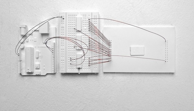
Photography of ceramics used in this document were made by Hanna Fuhrmann for the Hekmek exhibition. Making-of and high resolution images here. Free for personal use, ask for other purposes
This document covers embedded analysis techniques and tools. This is a resurrection of the Embedded Analysis node from the 27c3 with a few new techniques and observations added. Please feel free to contribute and edit religiously. The document is sectioned into finding Serial and JTAG debug interfaces which provides general techniques that may be modified to find additional interfaces, examining the aesthetics of the target for clues that indicate points to look for interfaces or how to narrow the search space and dumping memory.
All non-trivial abstractions to some degree are leaky
-- Joel on Software
This rule, generally applied in software development, is also relevant to hardware security, especially embedded security. Consider the abstraction layers between different fields of development that go into making a single device.
- Chip/ASIC designers
- PCB/layout designers
- Embedded software developers
Each field may require different debug interfaces. Each bring their own nuances and common design practices that influence the physical layout and look of the device. The aesthetics give clues as to interesting demarcation points between the layers to look at. For example, consider a security specification that requires a certain secure chip be placed under a layer of epoxy. The purpose of the epoxy is to make the pins of the chip difficult to probe and to make it difficult to remove. However, in the following example, you see a chip placed under epoxy but whose contacts are exposed through vias found on the bottom side of the PCB, making this measure near-moot.
 |
 |
|---|---|
| top | bottom |
Apart from a interface left mistakenly exposed in the design some interfaces are left intentionally for failure analysis when a broken devices returns from the field. These many interfaces might remain in the board design until some time has past, in the order of years. In the best case debug interfaces, pads, vias, traces, are removed after this time has passed and reliability of the specific hardware design has proven itself enough that the designers feel comfortable removing the interfaces in later board revisions. (E.g. Amazon's Echo had JTAG and a SD interface that was removed many years later in revision 3.) In the worst case, and more often then not, the existence of the interface gets lost in an abstraction layer and remains. Further, there seems to not-enough cost-to-benefit understanding of repair-ability vs security. Oddly, to this day (late 2018), there is an very odd silence in the room when you suggest to a design firm to write down an upper threshold of the number of devices that could ever possibly brick in the field, suggesting that you (or your client) are prepared to cover the cost if they just remove the damn JTAG.
I digress.
This is a living document intended to provide a reference on embedded device security analysis, from the hardware design, exposing debug interfaces wherever they be and dumping memories where they lay, with some foray into firmware examination.
License
Except for a copyright on the ceramic photographs made by Hanna Fuhrmann, there is no copyright on this text or its content and you are welcome to contribute to, or cut+paste for any commercial or non-commercial use, with or without attribution. The authors and contributors only ask that you remember us fondly when we are old and poor. Also, if you do wish to use the ceramic photographs for something other than personal use feel free to ask (hi-res here).

Many of the tools and techniques discussed herein use a microcontroller to communicate with a targets pins. It is important that both (microcontroller and target) use compatible voltage levels. For example, if the tool you choose is Arduino based these are typically working at 5v with some offering 3.3v. Raspberry Pi's GPIO drive at 3.3v. If the target interface you are searching for or the target memory chip you are dumping operates at 1.8v you will need to place voltage shifters between your tool and target pins. Options for voltage compatibility are discussed in the Voltage Shifting Appendix in greater detail.
If you think about serial and embedded devices the first thing that comes to mind is probably a serial console on home routers. Such consoles might provide means to configure and debug the device. But serial is used for much more. You will find serial used between a baseband processor and the primary CPU to send AT modem commands. It might be used to programming the memory of a micro-controller or DSP, and much more.
Often when a serial console is intentionally left on the target board you will find it on 4 pins or pads found next to each other in a row (Gnd, RX, TX, VCC). There is likely no surer way to excite a security analyst that including 4 contact points in one row on a board. Both RX and TX pins in HIGH VCC when left idling. The reverse is true, in the less common inverted Serial mode, with both being in LOW VCC (0v).
When looking for Serial manually you will usually want to first see if there is an active serial console where information may be printed during boot. Checking for this usually means choosing a common console baud rate such as 115200 and checking each candidate contact point on your target with the RX pin of your serial cable. Remember to restart the device every once in a while. Devices that print information during initialization may not be as active, if at all, after the device is fully initialized. Also, consider the expected serial voltage of your target and be sure the USB to Serial converter you are using communicates at this voltage.

RS232enum (code) is a Arduino based program that can be used to scan and find serial on 30+ pins, vias (through-holes) and pads. First you should determine the set of pins to scan. Checking the voltage level of all possible target pins, pads and vias can help reduce the set. Serial will be commonly found at +/- 3.3v, 5v and sometimes +/- 12v VCC. 3.3v is a very common TTL level found in embedded electronics so this characteristic in itself does not indicate serial. To scan the pins you will connect an Arduino with the RS232enum sketch to the target set of pins so make sure your Arduino I/O supports the same voltage as your target pins (see Voltage Shifting Appendix). Connect your Arduino to the target pins and load the sketch onto your Arduino and then open a serial console at 115200 buad.
There are 3 basic scans that will be run:
Passive Parallel
Passively monitor all attached pins/vias/pads for 4 seconds. When the state (1 or 0) changes print "active" pins to the console. Note: active pins might indicate an RX pin or it might indicate some other interface. Example output below shows activity but not enough to indicate serial:
 -> passive_parallel_scan(4000000)
    PIN35=1  PIN27=1  PIN29=1  PIN31=0  PIN33=1  PIN33=0  PIN33=1
    PIN33=0  PIN33=1  PIN33=0
Active Parallel
For each pin the code will choose one as candidate TX pin and send a wake-up
signal (such as a carriage return 0x0A \n) at various baud rates. Pins
that show activity accurately indicate the RX and TX serial pin. Below is
example results showing potential serial activity when a 0x0A is sent at
baud 115200 with TX set to PIN33 with active output showing on pin PIN27
indicating it likely the RX pin:
 -> active_parallel_scan(4000000)
    baud: 9600
    0x0A -> PIN35:	PIN33=1
    0x0A -> PIN27:	PIN40=1
    0x0A -> PIN37:	PIN27=0  PIN40=0  PIN27=1
    [...]
    baud: 38400
    0x0A -> PIN35:	PIN40=0
    0x41 -> PIN35:	PIN40=0
    0x41 -> PIN27:	PIN40=1
    0x41 -> PIN37:	PIN40=0  PIN27=1
    [...]
    baud: 115200
    0x0A -> PIN33:	PIN27=1  PIN27=0  PIN40=1  PIN27=1  PIN27=0
    PIN27=1  PIN27=0  PIN27=1  PIN27=0  PIN27=1  PIN27=0  PIN27=1
    PIN27=0  PIN27=1  PIN27=0  PIN27=1  PIN27=0  PIN27=1  PIN27=0
    PIN27=1  PIN27=0  PIN27=1  PIN27=0  PIN27=1  PIN27=0  PIN27=1
    PIN27=0  PIN27=1  PIN27=0  PIN27=1  PIN27=0  PIN27=1  PIN27=0
    PIN27=1  PIN27=0  PIN27=1  PIN27=0  PIN27=1  PIN27=0  PIN27=1
    PIN27=0  PIN27=1  PIN27=0  PIN27=1  PIN27=0  PIN27=1  PIN27=0
    PIN27=1  PIN27=0  PIN27=1  PIN27=0  PIN27=1  PIN27=0  PIN27=1
    PIN27=0  PIN27=1  PIN27=0  PIN27=1  PIN27=0  PIN27=1  PIN27=0
    PIN27=1  PIN27=0  PIN27=1  PIN27=0  PIN27=1  PIN27=0  PIN27=1
    PIN27=0  PIN27=1  PIN27=0  PIN27=1  PIN27=0  PIN27=1  PIN27=0
    PIN27=1  PIN27=0  PIN27=1  PIN27=0  PIN27=1  PIN27=0  PIN27=1
    PIN27=0  PIN27=1  PIN27=0  PIN27=1  PIN27=0  PIN27=1
    [...]
Active Per-Pin
This is similar to Active Parallel except that each RX pin is checked individually. Example output shows likely serial (TX=PIN33, RX=PIN27):
 -> active_per_pin_scan(4000000)
    tx:PIN35 rx:PIN27 baud:9600
    0x0A -> PIN35:	PIN27=1  PIN27=0 PIN27=1  PIN27=0  PIN27=1
    PIN27=0  PIN27=1 PIN27=0
    [...]
When an active pin(s) is found, connect a serial cable to explore further. It is useful to have an RS232 to USB breakout cable or board. Be sure to have one that operates at your targets voltage (e.g. 3.3v or 5v and some are switchable).

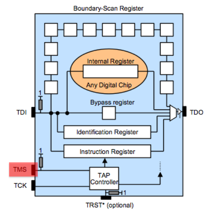
JTAG can be used to debug running software, check the health of solder joints, check connectivity between IC's and checking or setting the state of pins on a JTAG enabled IC. JTAG IC's can be chained together so that one bus (set of pins) can be used for all of them. There are 4 pins required. TDI (input) TDO (output) TMS (state machine) TCK (clock). TDI and TMS require a pull-up resistor between 1k and 10k. More commonly 4.7k is used and if you find such resistors on your board these and neighboring contact points are good places to start scanning.
How it works
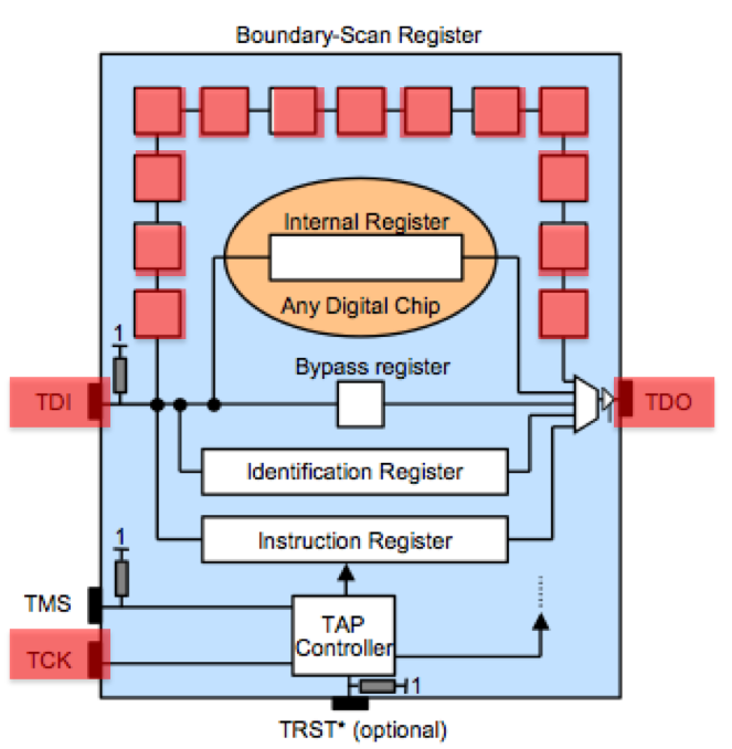
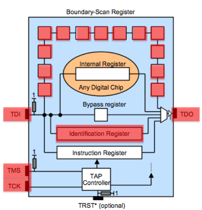
JTAG has 4 required lines. TMS, TCK, TDI, TDO. A 5th TRST is optional. JTAG has a state machine called the TAP. The JTAG TAP has very simple logic that controls what "register" is active between TDI and TDO (input/output). The JTAG spec defines that by default the IDCODE or BYPASS register will be between input and output. The TCK/clock line shifts bits out of the current register like a shift register or FIFO buffer. To change the register between TDI and TDO the TMS pin is used. The TMS pin controls the TAP. Finally, the optional TRST line resets the TAP when toggled.
 |
 |
 |
|---|---|---|
| The JTAG registers and lines (pins) | Input line | Output line |
 |
 |
 |
| Clock line | State machine line | Provided the ID register (IDCODE) is the default on reset we only need to toggle TCK and read the output on TDO |
 |
 |
 |
| The Boundary-Scan register can be used to check the state of pins and internal registers (defined in the target chips BSDL file) | If we provide input on TDI we can also set the state of pins and internal registers of the boundary scan, in addition to reading current state | The TMS line is important for being able to switch between different registers. |
 |
 |
|
| Hence, the reasoning behind the 4 JTAG lines | Several JTAG enabled chips can be chained together on the same lines. In this example the first is set to access the Boundary Scan register, and the second is set in BYPASS mode |

JTAG scanning tools assume that the target chip(s) are in one of two possible
default states. Either the IDCODE state or BYPASS state. In the IDCODE state
the chips IDCODE register will be the default register attached to the TDO pin
(output). So if you were to monitor the TDO line and clock the chip (TCK) 32
times you should see a valid IDCODE on the output. In the BYPASS state the
BYPASS register will be set between TDI and TDO. In this mode you can clock
(TCK) into the chip (TDI) a known bit pattern and check for it on the output
(TDO). The scanning tool you choose will likely attempt these possible states,
or attempt to place a chip into one of these states (through use of the TMS
line) with every possible pin combination you connect.
Scanning Tools
| Tool | Links | Platform | Pin max | Voltages |
|---|---|---|---|---|
| JTAGenum | code/docs | C Arduino RaspberryPi Odroid-X4U | 13 to 46 | 5, 3.3v, (experimental 1.8v) |
| Dumb and simple. Number of pins dependent on Arduino (Teensy++ for 46) or RaspberryPi (26 by default). Arduino's available in 3.3v or 5v versions. RaspberryPi 3.3v. Odroid X4U for 1.8v. Or see Voltage Shifting Appendix for voltage level shift configurations | ||||
| SWDscan and JTAGscan | SWDscan code/docs JTAGscan code/docs | C Arduino SWD finder and JTAG finder | 13 to 46 | 5, 3.3v |
| SWD scanning but also the JTAG scanner using logic similar to Jtagulator | ||||
| JTAGulator | code/docs | Parallax | 24 | 1.2v, 1.8v, 2.5, 3.3v |
| Board is designed for this task and provides support for low voltages without requiring voltage shifters | ||||
| JTAG Finder | code/docs | AVR microcontroller | 13 to 46 | 5v, 3.3v |
| This was one of the first (if not the) JTAG scanners. People that don't care for Arduino may prefer this solution. Same voltage considerations required as with JTAGEnum. | ||||
| Commercial Products | ||||
| There are various commercial WYSIWYG GUI products that now offer JTAG scanning functionality such as MiracleBox, JTAGfinder, EasyJtag. Most of these are designed for specific targets, most of which are phones. For other targets these products add an abstraction layer you will have to traverse if you want to actually connect to the JTAG port of your target. They can still be used to find the JTAG pins on unsupported targets and provide the targets IDCODE. | ||||
Apart from the default JTAG state requirements that help guide automated scanning, electrical requirements for the pins can be used to determine the JTAG pin layout by hand, at best, or at least help determine which pins are likely to contain JTAG allowing a reduction of the total set targeted for scanning. Therefore understanding how to find JTAG by hand can also assist in the setup for automated scanning.
Certain JTAG pins must have a default HIGH or LOW state. This is important so that when nothing is happening on the bus, and the JTAG TAP state machine should be idling, that the natural electrical fluctuation of pins left floating do not confuse the state machine. For example, if the TMS pin that determines the state of the JTAG TAP and the TDI and TCK pins are all floating somewhere between HIGH and LOW there is a slight chance that the chip could be inadvertently be placed into a state that interrupts the normal operation of the system. To avoid this pins are set into a default state which is facilitated using a pull-up or pull-down resistor to the pins line (pull up means resistor connected to pin and VCC, pull down means resistor connected to pin and ground). Nearly all specifications recommend using resistors between 1k and 10k with many found implementations using 4.7k or 10k. The common pull-up/pull-down recommendations are given below. These are based on ARM recommendations and you can find additional specifications from other vendors in the Vendor JTAG Specifications Appendix.
- TCK - pull down LOW (recommended)
- TDI - pull up HIGH (recommended)
- TDO - pull up HIGH (recommended)
- TMS - pull up HIGH (required)
- TRST (optional) - pull up HIGH (required)
You can measure if a pin has a pull down by checking the level of resistance (using a multimeter) between a target pin and ground. Ground is common and can be found on metallic plates over chips or even the metal of a device's case. To determine pull up resistance you will need to determine the VCC line of the chip first. In fact, you may need to find the VCC Vref line typically found among your target JTAG set of pins. This sounds harder than it is in practice.
To find the Vref line you will want to find all the pins of your target set that are in the default HIGH state when the device is on. What voltage is HIGH? 3.3v and 1.8v are decent assumptions. As a rule of thumb though the HIGH voltage will have at least 3 pins in this state as 3 of the JTAG lines are required to be in this state. If the JTAG port includes a Vref pin that would mean 4 pins in HIGH state would be found. To find the Vref pin choose a pin as the Vref candidate from the set of HIGH pins and measure the resistance between it and the other pins. Do this for each candidate. Vref will be the pin where the other pins in the set hold a common resistance value to it in a range between 1k to 10k. (Warning: this technique to find the Vref/Vcc pin has worked for me as much as it has failed.)
In the process of determining the Vref pin you will have now removed that pin from the possible candidate pins that could be TDI, TMS or TMS (by default HIGH). Later we will use what we understand of JTAG's default states (IDCODE or BYPASS) to define them more accurately but for now let's move to finding the TCK pin with a default state of LOW. To find the TCK pin measure the resistance to ground of all pins at or near 0v during normal device operation. Ideally, you will find one pin with a value between 1k and 10k. If this is not what you find, perhaps the processing of checking helped remove some pins as TCK candidates. For example LOW pins whose resistance to GND is low (under 200k) or very high (over 1M).
To "find" JTAG now we can use a common JTAG cable and connect only the required lines based that are determined by which default TAP state (IDCODE or BYPASS) we are testing first. Assuming the chip is in the IDCODE state, meaning the IDCODE register is already attached to TDO, we only need to know the TDO line and TCK line, ignoring the other pins. Assuming your search resulted in only one TCK candidate line testing is easy as with TCK know you only need to find a single pin, TDO. Now you can manually connect the TDO line of your JTAG cable to each of the 3 HIGH default lines from before. Connect each and execute your JTAG software (OpenOCD for ARM, MIPS targets) and attempt each line.
If your target chip is in the BYPASS state by default finding JTAG will require determining the TDI line in addition to the TCK and TDO lines. If we started with 4 HIGH lines and 1 LOW line, and we already determined 1 of the HIGH's to be Vref, and we know the LOW is TCK and the 3 remaining HIGH must contain TDI and TDO lines. In this scenario you will have to try 6 different arrangements for TDI and TDO to find JTAG. You will also not be able to use common JTAG software and may need to use JTAG scanning software to send a predetermined pattern through the BYPASS register. (or, perhaps someone can whip up an OpenOCD script)
In its most primal form JTAG provides very basic functions such as reading the IDCODE and checking the Boundary scan register. But many chips provide additional functionality including debugging code running on the chip (On Chip Debugging). If you are lucky a BSDL file (Boundary Scan Definition Language) can be found for your target which defines most of the known OCD instructions. But more often than not the instructions are not documented. In-fact it is so common that some chip analysts have mistaken hidden instructions as evidence of a hidden chinese backdoor. But there are ways, when you have time and patience, to deduce instruction functionality through educated brute force.
At the 26c3 Felix Domke "tmbinc" describe how to use telepathic examination of the Instruction Register to determine higher level JTAG functionality (lecture video, paper / cache). In his case he used this to find an undocumented bus. JTAGenum provides some basic functionality for enumerating the Instruction Register. This is not a passive technique. In the source repository, you will also find OpenOCD scripts to enumerate instructions.

FLASH memory come in various forms. SPI, NOR, NAND and eMMC are common types. Each come in TSOP or BGA packaging.
- SPI FLASH is access through a serial interface with a few pins
- NOR is simple and has separate pins where address is supplied and pins where data comes out. The pin count can be up to 46 pins. The pin map can differ between chip vendor.
- NAND has 8 or 16 pins that both address input and data output are multiplexed across using a protocol. The pin maps for both BGA and TSOP are pretty standard across vendors.
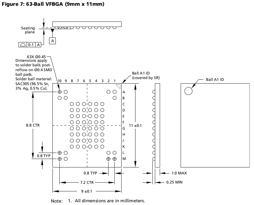
- eMMC is basically NAND inside but includes a controller results in the interface operating like an SD card with 4 to 11 pins required. The BGA pin map is standard across vendors depending on the BGA package size.
The process of dumping memory will involve removing the chip from the board. In some cases such as with SPI and in some situations with eMMC it may be possible to dump in place (aka ISP). When removing the chip you will place it in a breakout board in order to connect to a reader. All of this will be covered in the following sections.
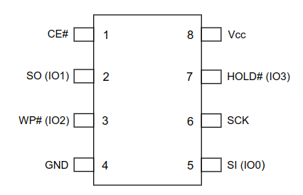
SPI FLASH memory has a simple serial interface that can be dumped using the Flashrom.org software and a RaspberryPi. The memory can be dumped with chip remaining in place but target device off, with power provided from the Raspberry Pi. Alternatively if issues persist remove the chip from target and connect directly to RaspberryPi.
Common SPI FLASH pins:
You may first check that Flashrom.org software supports your target chip by reviewing the Support Hardware list. If your chip is not supported it still may be possible to dump the chip by modifying the code or using a similar target chip.
Connect SPI pins to the Raspberry Pi pins:
- 25 GND
- 24 /CS CE
- 23 SCK
- 17 VCC+HOLD+WP
- 21 MISO = master in = slave out ("so/do" of target)
- 19 MOSI = master out = slave in ("si/di" of target)
Be sure the Raspberry Pi with SPI enabled using either raspi-config or making certain in /boot/config.txt contains dtparam=spi=on.
On the Raspberry Pi install flashrom either from sources or apt-get.
Execute:
flashrom -p linux_spi:dev=/dev/spidev0.0,spispeed=1000
or
flashrom -p linux_spi:dev=/dev/spidev0.0,spispeed=1000 \
      -r dump.bin -V -o log.file2 \
      -c MX25L3206E/MX25L3208E
Setting spispeed=1000 is for 1Mhz. Lower if having issues. If you are using voltage stepping up or down it may be important to slow this value down. Take several dumps and compare their output. Also pay attention to voltage drop messages in RPi dmesg. Be sure you are giving RPi enough power.
NOR uses a separate address and data bus (separate address and data pins) to access memory. The Parallel Flash Dumper code, loaded onto an Arduino or compiled on a Raspberry Pi, is used to dump the memory to the serial console at 115200 baud.
The following breadboard layout shows (made with Fritzing, sketch/source) an Arduino board connected to a FLASH chip with 23 address pins and 16 data pins. The setup using a Raspberry Pi would be similar. Shift registers are used to take one line of the Arduino and turn it into 23 address lines (serial to parallel shift registers) and take the 16 data lines and convert it back into bytes sent across another Arduino line (parallel to serial shift registers). To desolder and remove a TSOP FLASH chip from your target see this video.
 |
 |
The code might need to be modified depending on the order and specifics of the state pins for your target FLASH chip. The following image shows the order and state for a Spansion FLASH chip. The minimum timing specifications (tRC, tACC, etc) are not important. What is important to note is that, in this example, RESET# and WE# are pulled high first, the the address is sent, then CE# and OE# are pulled low, then data is read.

You will also need to know where the address, data and state pins are on the chip. Likewise this is found in the datasheet.

Unlike NOR where address and data have different pin sets, NAND has either 8 or 16 pins that both address and data share. To multiplex these pins the standard ONFI NAND protocol is utilized. The Arduino based NANDDump can be used to dump NAND memory. I have not had a chance yet to provide a more friendly introduction to dumping NAND but please feel free to contact me for help.
Briefly, determine first target chip bus width, package type and pin spacing, voltage:
Later when troubleshooting code, know that you can communicate with the chip as slowly as you like. Most hardware designers want to read and write to memory as fast as possible so the timing requirement markings found in the datasheets read/write diagrams determine the maximum rates. For example the tACC marking the diagram below is 10ns which means that after sending the address the data will be ready after 10 nanoseconds. For our purposes of reading memory out, quite slowly in comparison, we can ignore all of these timing markings.

To be certain this assumption is correct, quickly look over the timing specification table in the datasheet (that clarifies what "tACC" means) and confirm that all values specify the minimum amount of time to wait, and that none specify a maximum time.
Increasingly more devices are using eMMC memory. This is basically NAND memory with the memory controller integrated into the chip. eMMC can be thought of as an SD card as they share protocol and required pins. eMCP is similar but this adds RAM as well with its own pins for RAM which can be ignored.
todo: include images of common footprints for different BGA package sizes. Describe how to use an SD card, SD reader and tools such as the Riffbox.
I will at some point write this up but the method for TSOP desoldering is rather simple. You can use a heat gun if you like but the simplest method is to just add gobs of solder to both sides of the chip so that when you heat up the solder one side can be lifted off the board. This process is easy to see in this video:

http://vimeo.com/11699576
Once you have the chip out of the board you will clean the solder off of the pins with solder wick and then place it into a breakout board. The breakout board you use needs to match the width of the chip and the spacing between the pins (0.5mm, 0.8mm). Here are some boards I've used:
Breakout Boards
- Conrad SMD-Adapter multiboard 0.40 0.50 0.50 0.65 0.80 1.27 mm. Also search for "pcb smd"
- Distrelec "Prototyping Boards" of various sizes
- microcontrollershop boards of various sizes
- Reichelt "SMD-Laborkarte" "SMD-TSOP" 0.4mm 0.5 0.65 0.8 1.27 multiadapter also see their whole list of Laborkarte SMD-Adapter boards
An exhaustive list of alternative options and methods can be found in this older document MemoryBreakouts.pdf
A BGA chip can be extracted with a heat gun, hot air station, rework station or IR rework station. These can reasonable cost between 20 for a basic adjustable heat gun to 800. Heat is applied to the location of the chip until the chip can be tapped out of place. From experience the most valuable upgrade to be had over basic heat gun is adding and using a preheat plate. Many rework stations come with a preheat plate or one can be purchased separately or self-made with a ceramic tile (see minute 13:41 for Ben Krasnow's self-made plate). A preheat plate helps reduce the chance a trace is pulled from the PCB in the process, or that the target chip is destroyed. Before applying heat directly to chip the entire board or target is placed over the preheat plate and brought to a temperature below the point of melting solder (180°C 370°F) and after this heat is then applied directly to chip area to melt the solder. Some rework stations come with temperature measurement sensors but having a inexpensive IR Thermometer can be helpful.

https://youtu.be/XRYkZTIbvUA
Once the chip is removed from target it should be cleaned of solder and residue using solder wick and flux, and then further cleaned with alcohol. The clean chip can be prepared for placement into a breakout board.
The breakout board chosen needs to match the physical properties of the chip. So if the targets chip has pads that are 0.8mm spaced apart then a breakout board with this spacing should be acquired. The breakout board should also support the footprint of the target chip. E.g. for a NAND chip that is 11 x 9 pins the breakout board should have the same grid. It may be possible to reduce the total grid size of some of the outer rows on the target chip are not required. E.g. FBGA NAND only has active pins in the center which reduces the total grid required down to 8 x 6. A list of locations you can purchase breakouts can be found in the Breakout Boards TSOP section above.
To prepare the chip for placement into a breakout board BGA balls can be pushed into place by hand and needle using some flux paste to hold them in place and a magnifying light if available. See this image for more detailed instructions:
Alternatively the breakout board could be prepaired first rather than preparing the chip. To avoid BGA balls moving out of place place the airflow of the heat gun to the lowest possible setting or heat the chip or breakout board from the back-side.
Additional Resources
- Stackexchange thread on SMD rework temperatures
- Mikrocontroller thread 2009 (German) on rework stations and desoldering BGA chips (archive)
- ~20EU Tacklife T04 IR thermometer
- ~800EU AOYUE Int710 IR rework station with preheat plate and foot peddle is nice but not necessary
- ~300EU PUHUI T870A IR rework station with preheat plate is a good value
- ~150EU AOYUE Int968 hot air soldering station (no preheat) is a very good value but you will have to get a preheat plate seperately (see minute 13:41 for Ben Krasnow's self-made plate) or preheat around the target using the heat gun placed at a further distance from target before switching to directed heat on target chip.
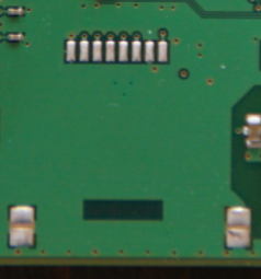
Additional clues can be found with a discerning eye toward the aesthetics of the layout and seemingly quaint elements of the target. Particular attention should be given to the style and cluster of pads/vias/pins and markings for missing connections. For instance, pads which have slight indentations perhaps indicate that they were used in a bed of nails tester commonly used for automated quality assurance testing during manufacturing. If a small set of vias have solder left on them while others do not it is an indication that 1. they are related to each other 2. they are likely used for some form of testing or debugging.
| Missing connectors | ||
|---|---|---|
 |
 |
 |
| RJ45 connector | FLASH socket | SD slot |
Traces on the PCB of the target between various components may provide clues as to the purpose of pins or pin sets. For example in this video tutorial an aesthetic clue provided in the form of some pads having solder already, in addition to tracing, leads to determining the JTAG header cluster.
Typically an image editor that supports layers such as GIMP or Photoshop are used to trace lines between layers. Images are taken of top and bottom of the target board and then aligned in the image editor. For example the "Handle Transform Tool" in GIMP makes aligning easy. Some years ago we wrote the tool DePCB specifically for the purpose of manually tracing but for most tasks GIMP or Photoshop will suffice.
| top | bottom |
|---|---|
 |
 |
The tools you use to interface with debug ports or memory chips will need to "speak" at a compatible voltage of the target. If you are using tools that already have built-in voltage regulation support for I/O (such as the JTAGulator) this may not be of a concern. If you are using an Arduino, RaspberryPi, AVR, etc, you will need to take care. Check first the voltages across the target pins, memory or target components you intend to interface with. Get an idea of their likely minimum and maximum voltages.
For 3.3v and 5v targets, you can use either Arduino or RaspberryPi without modification. Some Arduino boards are switchable between 3.3v and 5v. For 1.8, 1.6 or voltages higher then 5 I'd suggest these options in order of complexity:
- Build a specialized voltage regulation shield. The inputProtectionShield made by Dylan Ayrey was built and tested with JTAGenum. An additional fork if Dylan's shield has been built and tested by dipusone inputShieldProtection
- Cheap 4 or 8 pin bidirectional shift boards, as shown in image below. These
can be found at Sparkfun US/EU,
Pimoroni UK/EU, Adafruit
US, and others. For this arrangement,
you provide a reference voltage to the LOW side of the shifter which matches
your targets requirements and use the VCC pin from your Arduino as the
reference voltage for the HIGH side. For a reference voltage you can use a
cheap lab power supply or any other device that supplies the same voltage
with enough amp (500mAh should suffice.) Note: a Teensy++ and other boards
that have been modified and stepped down from 5v to 3.3v will not be able to
drive more than 8 pins. So you may need to run your board at its native
voltage.

You can find cheap cables such as those from Amontec or can build your own. When you are scanning to find JTAG you may not need these. But when you want to debug the running software (OCD, on-chip-debugging) you will need one.
OpenOCD is open source software for interfacing with most JTAG cables and works well with ARM targets and some MIPS targets as well as a few obscure architectures. You can search in the /usr/local/share/openocd directory for hints of support for your target.
We have also had success with the relatively cheap J-Link cables which is also supported by OpenOCD but also comes with its own software that provides some broader support for MIPS targets though it is not open source.
When you have a dump of memory or even a firmware image, some basic techniques can help in analyzing before disassemble and code analysis.
Entropy is the randomness of data when comparing bytes with neighboring bytes. Entropy analysis code slides a window of N bytes across the data determining how different byte B is from byte B+1. This helps in determining if your target data is compressed, encrypted or reveals encryption keys and other distinctions within the data.
The python based Binwalk tool provides entropy graphs. Alternatively, others use libdisorder to generate graphs. The following shows several entropy graphs for different types a data created using libdisorder and gnuplot. See entropy_examples for more examples and code to generate these examples.
Examples
4MB JPEG

Random (''dd if=/dev/random of=random bs=1m count=4'')

Random Ziped. Notice common zip meta data cause larger Y scale

Random 4MB JPEG encrypted with RC2

Note that if you have a binary image or firmware image the compressed portions, encrypted portions and plaintext will become clearer as Y scales change.
Compression formats or file systems typically have static values in their header that may be noticeable in the data. Signature analysis software will search through a huge list of signatures and print offsets in your target data. Binwalk includes signature tools and there are standalone tools such as Signsrch via wine or sigscan osx/linux. The output will resemble:
0x00000000: ELF {
    machine: MIPS I
    class:   LSB
    bits:    32-bit
    type:    executable
}
0x00056b85: [type: data, len: 0004]  LZMA2
0x002772b0: [type: data, len: 0004]  JFFS2
0x00277598: [type: data, len: 0016]  SHA1
0x00279da0: [type: code, len: 1024]  CRC32
0x0027ac40: [type: code, len: 0120]  zlib
0x0027accc: [type: code, len: 0116]  zlib
0x002814fc: [type: code, len: 1024]  CRC32
0x002e7944 GZIP compressed data {
    name:      "main.bin"
    method:    deflate
    type:      binary
    OS type:   Unix
}
Or
the file loaded in memory is very big so the scanning could take many time

offset   num  description [bits.endian.size]
--------------------------------------------
002818fc 67   CRC-16-CCITT poly 0x1021 [16.le rev.512]
00279da0 83   CRC-32-IEEE 802.3 poly 0x04C11DB7 [32.le rev.1024]
002798a0 142  ACSS reverse sbox [..256]
00277598 307  SHA1 / SHA0 / RIPEMD-160 initialization [32.le.20&]
002716f7 309  padding used in hashing algorithms (0x80 0 ... 0) [..64]
002798a0 1198 FFT and FHT routines rv_tbl [..128]
00277cf0 1314 RawDES sbox1 [32.le.256]
00277af0 1316 RawDES sbox2 [32.le.256]
00277bf0 1318 RawDES sbox3 [32.le.256]
002779f0 1320 RawDES sbox4 [32.le.256]
002778f0 1322 RawDES sbox5 [32.le.256]
002776f0 1324 RawDES sbox6 [32.le.256]
002777f0 1326 RawDES sbox7 [32.le.256]
002775f0 1328 RawDES sbox8 [32.le.256]
00277598 1406 SHA1_DS [32.le.24]
0027accc 1525 zinflate_lengthExtraBits [32.le.116]
0027ac40 1529 zinflate_distanceExtraBits [32.le.120]
0027ac3d 1530 zinflate_distanceExtraBits [32.be.120]
00277598 1626 Lucifer (outerbridge) DFLTKY [..16]
0027216c 2257 unlzx table_three [16.le.32]
You can use the byte offsets and slice the file (dd is your friend) and attempt
to decompress or mount file systems. For example to attempt to uncompress the
GZIP segment that may have been found at 0x002e7944: dd if=targetfile.raw of=targetfile.002e7944.gz bs=1 skip=$((0x002e7944))
For some targets the serial interface may be inverted. To connect to these interfaces you can use a software serial interface or if your using a FTDI USB2Serial connector you can reconfigure the FTDI chip to invert RX and TX.
- To Change FTDI USB2Serial configuration. Set RX and TX lines to inverted with the FT PROG windows utility or on linux use ftx-prog or ftdi_prog. (alternatively the
ftdi_eepromutility that comes with libftdi:sudo ftdi_eeprom --read-eeprom /usr/share/doc/libftdipp1/example.conf. That will write eeprom toeeprom.new(filenamevalue in the conf file) but this is a binary file you must then modify and write back)
After connecting JTAG emulator to correct pins, steps to check if it is active or disabled
- Segger JLink with SWD target:
JLinkExe -device Cortex-M0 -if SWD -Speed 4000-
JLinkExe -device Cortex-M0 -if JTAG -Speed 4000 -AutoConnect 1 -JTAGConf -1,-1
(for supported-devicetypes see device list and use the same core name as listed, and see user reference) -
connect
expected result: Found SW-DP with ID 0xCHIPID -
halt
expected result:R0 = 20000093, R1 = 0000008F, R2 = E000E200, R3 = 0000008F R4 = 20002058, R5 = 00000000, R6 = 00026084, R7 = 00000001 R8 = FFFFFFFF, R9 = FFFFFFFF, R10= FFFFFFFF, R11= FFFFFFFF R12= 00000000 SP(R13)= 20003BF0, MSP= 20003BF0, PSP= FFFFFFFC, R14(LR) = 0000114F XPSR = 61000000: APSR = nZCvq, EPSR = 01000000, IPSR = 000 (NoException) CFBP = 00000000, CONTROL = 00, FAULTMASK = 00, BASEPRI = 00, PRIMASK = 00 FPU regs: FPU not enabled / not implemented on connected CPU.``` -
step,go,r savebin dump_0.bin 0x0, 0x1000000
- OpenOCD
-
interface jlink
#adapter_khz 40
adapter_khz 4000
transport select swd
proc attach () {
 init
 reset run
}
swd newdap ourtarget cpu -expected-id 0x{CHIPID}
# -irlen 4
dap create ourtarget.dap -chain-position ourtarget.cpu
target create ourtarget.cpu cortex_m -dap ourtarget.dap
#cortex_m dbginit```
-
While the general specifications of electrical characteristics and basic JTAG functionality is standard between vendors there can be some variations. Here is an archive of some vendor documentation concerning JTAG.
- ARM (full spec pdf, electrical only)
- Freescale MC56F827xx (full spec pdf, electrical only)
- Example: Cypress FX3 datasheet declares: "The JTAG TDI, TMS, and TRST# signals have fixed 50k internal pull-ups, and the TCK signal has a fixed 10k pull-down resistor"
