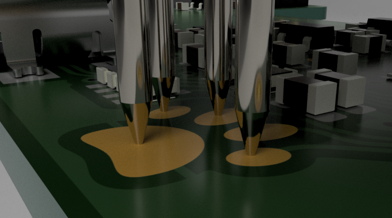
This is a project that aims to spice up the world of boring test jigs and programming headers with a completely new, full stack system for adding programming headers to your boards.
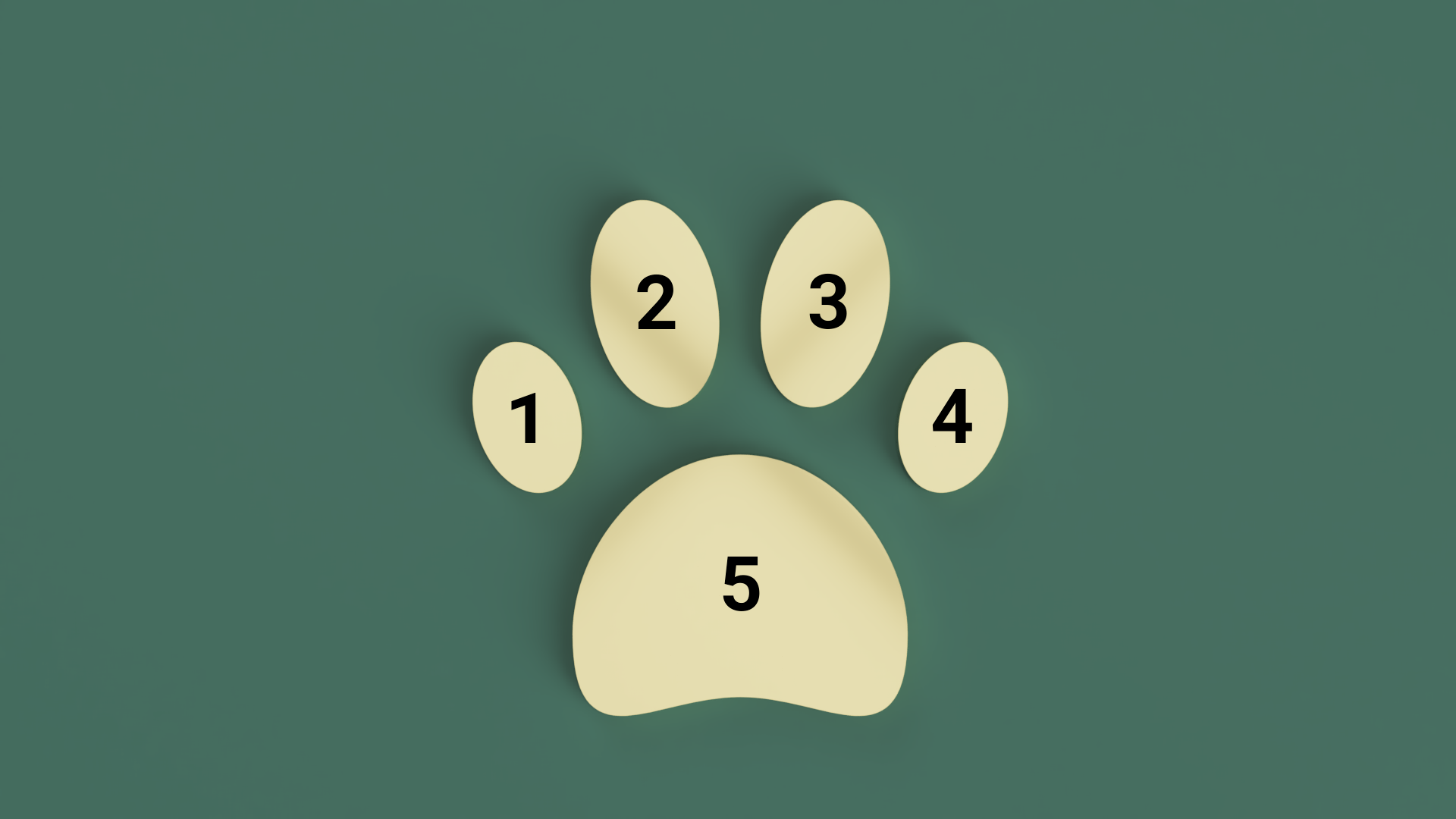
There are many benefits in the above shape compared to regular arrangements:
- No acid traps due to smooth curves
- No holes in the PCB means easier routing
- Big enough to solder wires to when needed, yet compact enough to be practical
- Large surface area makes it hard to peel the pads off and easier to hit with a jig
- Pretty
PawPad - contains the KiCAD footprint.
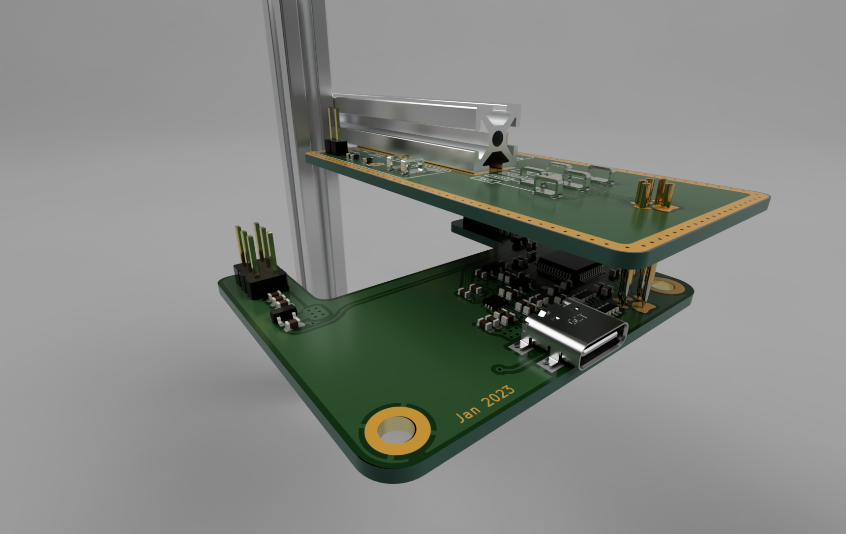
Programming Jig - contains a programming jig meant to be screwed onto a piece of 10x10 aluminium extrusion/makerbeam.
NOTE: this jig is not complete! It has not yet been tested for actual programming and may not be ideal!The pinout is standardized as outlined below:
| Pin | SWD | JTAG | SPI / ICSP | UART | I2C |
|---|---|---|---|---|---|
| Bean (1) | SWO | TDO | MISO | RX | - |
| Bean (2) | SWDIO | TDI | MOSI | TX | SDA |
| Bean (3) | SWCLK | TCK | SCK | - | SCL |
| Bean (4) | NRST | TMS | RST | RST | RST |
| Big Bean (5) | GND | GND | GND | GND | GND |
Did you add this to your PCBs? Let us know by opening an Issue!
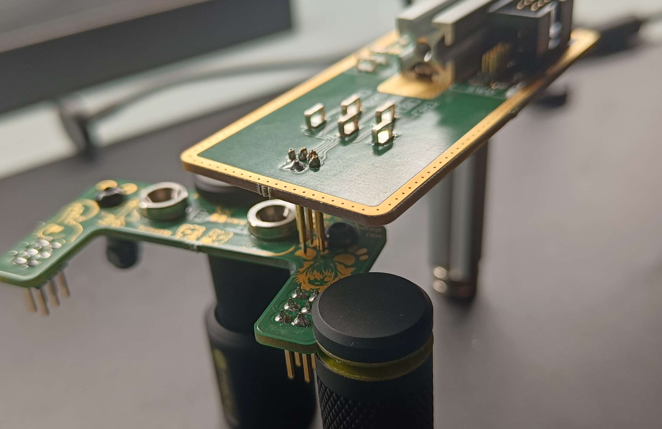
Example of the Programming Jig in action on a test PCB:
- Alternative designs with different numbers of pins
- Unified pinout standard
- OSHW certification
- Debugger design
This has been inspired by the original maker of the footprint, go check them out.


